LED/Key controller.
Chinese Titan manufactures numerous integrated circuits to control displays and keyboards, including the
TM1638.
This controller is the basis of some boards suitable for experimenting with microcontrollers and easily available in the WEB with really interesting
costs.
TM1638 has the following characteristics:
- Controls an 8 x 10 LED matrix
- Anode or common cathode display pilot
- Adjustable brightness - 8 levels
- 3 x 8 contacts scan input
- 3-wire synchronous interface, data/clock/strobe
It is similar to the TM1640, which allows you to control more displays and keys.
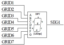
The typical common anode display application diagram is as follows:
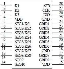
TM1638 is available in package SOP a 28 pin. The pinout is:
| |
Label |
Nome |
Pin |
Descrizione |
 |
DIO |
Data I/O |
26 |
Data input/output.
In writing, the data is transferred to the leading edge of the CLK.
At the exit, on the downhill side.
In transmission, it is an open drain and requires a pull-up. |
| CLK |
Ingresso clock |
27 |
Communication clock |
| STB |
Strobe |
28 |
Initialize the interface on the lower edge to receive instructions. The first byte after STB that becomes low is considered an instruction. When one instruction is processed, the other processes are blocked.
With STB at a high level, CLK is ignored. |
| K1-K3 |
Input keyboard scan |
1-2-3 |
Input of the data pins from the keyboard. Internal 10k internal pull-down |
SG1-KS1
SG8-KS8 |
Output (segments) |
5-12 |
Segment control output (P channel open drain) and key scan |
| GRID1-GRID8 |
Output (digit) |
24-19 |
N channel open drain |
| VDD |
power |
15
|
power + |
| GND |
common |
18
|
common gnd |
The data sheet states that the TM1638 can be fed up to 5V and can provide up to 50mA of sink current to the display segments.
The data sheet, in the queue, also contains some tables of electrical
parameters.
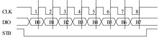
Communication interface.
Communication takes place over three wires:
- CLK : clock, from the Master
- STB : strobe, from the Master
- DIO : bidirectional data i/o
It is a synchronous communication: data from the microprocessor can be changed until the clock is low and read on the rising
edge.
The communication start condition is the application of a low level on the STB line.
When STB is at a high level, the TM1638 does not respond to any data or command transmission. This allows you to connect multiple TM1638s on the same clock and data lines, dedicating a separate strobe line to each one, similarly to the SS/CS signal of SPI communication.
The manufacturer's proposed diagram (see above) includes 10k pull-up on the communication lines and 100pF real mass capacitors, which are inserted to reduce noise in critical application environments.
In fact, the manufacturer designates the TM1638 as suitable for use in EMC-disturbed environments, such as household appliances and the like.
SPI?
The interface would seem to adapt to the specifications of an SPI communication, manageable through the MSSP module present in many microcontrollers.
The STB pin has a similar function to the SPI SS/CS: when communicating with the TM1638, STB must be at a low level. If the line is high, the chip will not accept any data.
For data transmission or reception, set the CLK pin to a low level, then set the DIO pin to the desired value and return the CLK pin to a high level. The transition allows the chip to capture the data.
However, in practice there are some big differences:
- A standard SPI interface has two lines for data, input and output (MOSI/MISO or SDO/SDI), while the TM1638 has only one bidirectional data line (DIO).
This could be corrected by combining SDO/SDI with DIO, but interposing a Schottky diode or a resistance between the DIO and SDO line, to isolate the condition at a high
level.
- Outgoing, the TM1638's DIO pin is an open drain and therefore requires a pull-up.
- The less significant bits are sent first, while in the standard SPI interface it is the opposite.
You need an SPI device that can reverse the output order.
For example, in C for Arduino and the like:
shiftOut(data,
clock,
LSBFIRST,
address)
If this option is not available, the bytes to be sent and those received must be sent 8
times.
The structure of the registers.
The TM1638 can receive commands and data, and communication involves a simple command/data structure.
The message sent to the TM1638 follows the rule that the first byte after STB has been low sent is intended as a command. This can be single or followed by one or more data bytes depending on the function selected.
A transmitted block is terminated by the STB line returning to a high level, and the following functions are
possible:
- Turn the display on/off and adjust the brightness of the display
- Select the data input mode, whether single-directed or auto-increasing address
- Write a byte to a specific address
- Write multiple bytes from an address
- Read the keys
Commands are processed directly, while data is sent to internal registers:
- There are 8 double registers (therefore a total of 16 addresses, 00h 0Fh), which correspond to
GRD8:1
pin signals.
- Each controllable array consists of 10 bits corresponding to the GRID-SEG combinations, at the crossroads of which the controllable LEDs are connected.
It is possible to write only one register (single register mode) or even several registers later (increased auto mode). As bizarre as it may be, the table proposed on the data sheet is
replicated:
| seg1 |
seg2 |
seg3 |
seg4 |
seg5 |
seg6 |
seg7 |
seg8 |
seg9 |
seg10 |
x |
x |
x |
x |
x |
x |
|
| b0 |
b1 |
b2 |
b3 |
b4 |
b5 |
b6 |
b7 |
b0 |
b1 |
b2 |
b3 |
b4 |
b5 |
b6 |
b7 |
| xxhL 4 bit bassi |
xxhU 4 bit alti |
xxhL 4 bit bassi |
xxhU 4 bit alti |
| 00hL |
00hU |
01hL |
01hU |
GRID1 |
| 02hL |
02hU |
03hL |
03hU |
GRID2 |
| 04hL |
04hU |
05hL |
05hU |
GRID3 |
| 06hL |
06hU |
07hL |
07hU |
GRID4 |
| 08hL |
08hU |
09hL |
09hU |
GRID5 |
| 0AhL |
0AhU |
0BhL |
0BhU |
GRID6 |
| 0ChL |
0ChU |
0DhL |
0DhU |
GRID7 |
| 0EhL |
0EhU |
0FhL |
0FhU |
GRID8 |
The table should be read as follows:
- 80 LEDs or segments are controllable
- These are organized in 8 arrays of 10, each dependent on a GRIDn line
- Each array has two bytes, each corresponding to an address inside the chip
- The bytes at even addresses (0,2,4, etc.) have 8 bits each corresponding to the possibility of controlling
8 LEDs (or segments)
-
Bytes at odd addresses (1,3,5, etc.) have only the first two bits (b1:0)
corresponding to LEDs/segments; the other bits are not used.
The data contained in the registers are scanned by the internal clock and control LEDs and connected
displays. The even address registers correspond to the lines SEG8:1.
Registers with odd addresses correspond to SEG10:9 lines (the remaining ones are not implemented and are at 0).
Where seven-segment digits are available, it makes sense to use the 8 bits of the first byte for the 7 segments plus the decimal point and use the two bits of the second byte to control other
LEDs.This is the common arrangement on Chinese modules, which generally contain 8 7-segment displays and 8 LEDs. Some of these easy-to-understand modules are presented below.
Of course, the TM1638 can be used to control any other LED configuration or segment configuration, such as point matrix displays or custom displays. In such cases, the display elements will match the register
bits.
The register content will be presented on the relative display with a multiplex using the internal clock (about 450kHz) and a variable and programmable duty cycle to adjust the brightness.
Note.
- TM1638 does not have decoding between data and segments, so bits sent at 1 correspond to segments switched on, bits sent at 0 correspond to segments switched off. A simple external lookup table must be used to convert the symbols you intend to present into the corresponding bit mask to be
displayed.
- When switched on, the display is off (low-power condition), but the registers are not reset and may contain random
values.
Comnand set.
In the first byte sent after the front of the clock with STB= 0, a command must be inserted.
Commands are groups of 8 bits of which bits 6 and 7 indicate the following
type:
| b7 |
b6 |
Comando |
| 0 |
1 |
Data management |
| 1 |
0 |
Display control |
| 1 |
1 |
Registers address |
If STB goes high during the transmission of a command, this command is invalidated (the commands and data sent earlier remain
valid).
The data processing commands are:
| b7 |
b6 |
b5 |
b4 |
b3 |
b2 |
b1 |
b0 |
Funzione |
Descrizione |
| 0 |
1 |
0 0 |
|
|
0 |
0 |
Read/write data |
Write data on display |
| 0 |
1 |
|
|
1 |
0 |
Read keys |
| 0 |
1 |
|
0 |
|
|
Addressing
mode |
Automatic increase |
| 0 |
1 |
|
1 |
|
|
Single address |
| 0 |
1 |
0 |
|
|
|
Test mode |
Normal mode |
| 0 |
1 |
1 |
|
|
|
Test mode |
Bits b0 and b1 must not contain 01 or 11.
Bit7:6 are the command identifier.
Bit 5:4 can be set to 0. For bits that are not indicated, it must be understood that these bits should also be set to 0.
However, by filling the empty spaces with 0, we have that the command "Normal
mode" has the same value as the command "Write data on
display" and "Automatic increase", so the table should be interpreted as
follows:"Write data on display".
- 01000000 0x40 the normal operating mode: this means that the byte sent below is a datum
towards the display, with the automatic increase in destination addresses
- 01000010 0x42 start the keys read
- 01000100 0x44 single address mode
- 01001000 0x48 test mode (internal use only)
There is no description of the "Test mode", but since it is cryptically referred to as
"(for internal)" it must be assumed that it is an aid for the chip function tests before release by
foundry.
Three operating modes (command 0x40 and 0x44) are possible:
- 0x40 with increasing address destination: if at the command we follow the address of a register, the next data will be sent progressively to subsequent addresses starting from the one selected.
- 0x44 with fixed destination address: if we follow the address of a registry at the command, the subsequent data will only be sent to this address.
- 0x42 with subsequent reading of 4 bytes encoding the status of the buttons
The register addresses with bit7:6 to 1 correspond to the controllable
LEDs.
In general, on tabs such as those shown below, the even addresses correspond to 7-segment displays, while the addresses are equal to the LED:
| b7 |
b6 |
b5 |
b4 |
b3 |
b2 |
b1 |
b0 |
Indirizzo |
Bit utili |
| 1 |
1 |
0 0 |
0 |
0 |
0 |
0 |
C0h |
8 |
| 1 |
1 |
0 |
0 |
0 |
1 |
C1h |
2 |
| 1 |
1 |
0 |
0 |
1 |
0 |
C2h |
8 |
| 1 |
1 |
0 |
0 |
1 |
1 |
C3h |
2 |
| 1 |
1 |
0 |
1 |
0 |
0 |
C4h |
8 |
| 1 |
1 |
0 |
1 |
0 |
1 |
C5h |
2 |
| 1 |
1 |
0 |
1 |
1 |
0 |
C6h |
8 |
| 1 |
1 |
0 |
1 |
1 |
1 |
C7h |
2 |
| 1 |
1 |
1 |
0 |
0 |
0 |
C8h |
8 |
| 1 |
1 |
1 |
0 |
0 |
1 |
C9h |
2 |
| 1 |
1 |
1 |
0 |
1 |
0 |
CAh |
8 |
| 1 |
1 |
1 |
0 |
1 |
1 |
CBh |
2 |
| 1 |
1 |
1 |
1 |
0 |
0 |
CCh |
8 |
| 1 |
1 |
1 |
1 |
0 |
1 |
CDh |
2 |
| 1 |
1 |
1 |
1 |
1 |
0 |
CEh |
8 |
| 1 |
1 |
1 |
1 |
1 |
1 |
CFh |
2 |
Note that the Master must in fact send the address plus bits7:6 to 1; consequently the value to be sent, for example, for address 0 will be C0h, the value for the last address, 0Fh, will be
CFh.
In single increment mode, after the command you must send the address to which to write and the relative data.
In auto-increase mode, the starting address and data must be sent in succession; any amount of data can be written up to the filling of the
registers.
By default at reset (supply arrival) the selected address is 00h, i. e. the first digit on the left.
It is possible to write any number of registers.
If an address higher than 0Fh is sent, it is ignored and there are no effects until a valid address is
sent.
After the power supply voltage has been applied, the register content is not zeroed, so there will be segments/LEDs switched on in random combinations; you can reset the content by writing 0 in all sixteen
registers.
The commands relative to the display control concern its on/off status and the change in brightness, obtained with a PWM.
| b7 |
b6 |
b5 |
b4 |
b3 |
b2 |
b1 |
b0 |
Funzione |
Descrizione |
| 1 |
0 |
0 0 |
|
0 |
0 |
0 |
Luminosità |
PWM 1/16 |
| 1 |
0 |
|
0 |
0 |
1 |
PWM 2/16 |
| 1 |
0 |
|
0 |
1 |
0 |
PWM 4/16 |
| 1 |
0 |
|
0 |
1 |
1 |
PWM 10/16 |
| 1 |
0 |
|
1 |
0 |
0 |
PWM 11/16 |
| 1 |
0 |
|
1 |
0 |
1 |
PWM 12/16 |
| 1 |
0 |
|
1 |
1 |
0 |
PWM 13/16 |
| 1 |
0 |
|
1 |
1 |
1 |
PWM 14/16 |
| 1 |
0 |
0 |
|
|
|
Display
on/off |
Display OFF |
| 1 |
0 |
1 |
|
|
|
Display ON |
The table is not very clear and, in fact, it results that bit3 on/off must be added to the brightness value. So you have that:
- 10000000
0x80
display off
- 10001000
0x88
display on with PWM 1/16
- 10001001-100001111 0x89-0x8F 7 additional brightness adjustment
steps
After applying voltage, the display is off, which is the lowest power consumption condition.
To illuminate the active segments, an on command must be sent with the desired
brightness.
Once an addressing mode or brightness value has been programmed, they remain set until they have changed from a different control or the power supply has been switched off.
Read the keyboard.
TM1638 support 3 blocks of 8 contacts each.
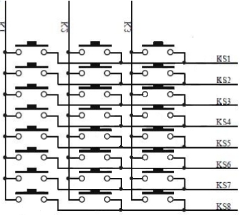
The keys are connected to three common keys (K3:1) and 8 lines (KS8:1), common with the segment command (SEG8:1).
The key condition can be requested by sending a specific command (0x42), followed by an 8-bit reading loop.
The lowest bit (bit0) is transmitted first.
In data output, the DIO pin of the TM1638 is configured as open drain and therefore requires an external pull-up.
The bytes read encode the buttons as follows:.
| b0 |
b1 |
b2 |
b3 |
b4 |
b5 |
b6 |
b7 |
|
| K3 |
K2 |
K1 |
- |
K3 |
K2 |
K1 |
- |
| KS1 |
KS2 |
Byte 1 |
| KS3 |
KS4 |
Byte 2 |
| KS5 |
KS6 |
Byte 3 |
| KS7 |
KS8 |
Byte 4 |
Basically, bits b2:0 and b6:4 of each byte are significant.
Keyboard scanning is performed automatically by the TM1638 without user control. Users only need to read key codes according to the time sequence. It takes a display cycle for keyboard scanning and a display cycle takes about 4.7ms. During this time, if two different keys are pressed, the key code read in both cases is that of the key pressed first.
Multiple keys belonging to the same line can be pressed (KSn): for example, for K1 and KS8, K2 and KS8, K3 and KS8 at the same time, bits 6:4 of the fourth byte are at 1. Buttons with the same K are not allowed, but on different KS.
There are several ways of connecting the keys:
The data sheet shows a diagram for scanning the keys:
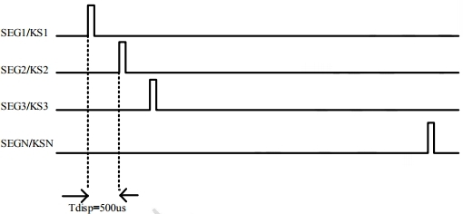
Scan between KS takes about 500us, depending on the chip clock.
When reading the button status, a wait time of at least 1us must be entered between the 0x42 command (key reading) and the subsequent bytes
read.
The management of registers.
The management of the registers involves a simple command/data structure.
Let's see in the following diagram an example of a simple, self-addressing, incrementing transmission of
commands:
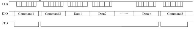
The first transmission includes a single command for setting the addressing mode (in this case self-increasing). STB is low at the start of transmission and returned high at the end of transmission.
Command2 contains the starting address and is followed by the transmission of the desired number of data. STB at a high level closes the transmission.
Command3 is a simple command, such as brightness adjustment.
- Command1 set display mode
- Command2 send start address and n Data
- Command3 set brightness
See also operating examples below.
If we write to individual addresses, each command/data group is separated from the next one by the strobe.
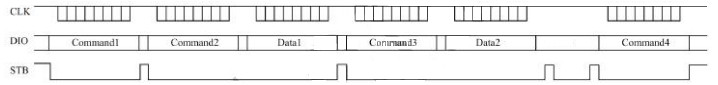
- Command1
set display mode
- Command2-Data1 send address and data
- Command3-Data2 send address and data
- ....
- Command4 set
brightness
See also operating examples below.
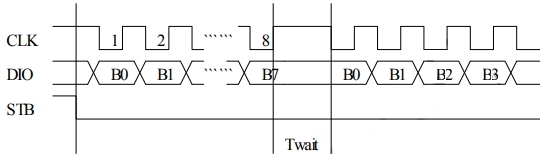
When writing a byte, these timings must be respected:
Data is acquired on the rising edge of the clock. To read the button status: 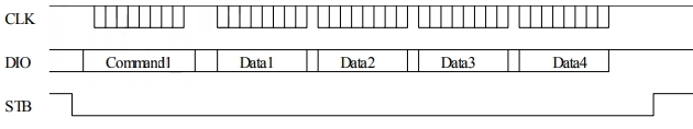
- Command1 set key
read mode
- wait 1us min.
- Data1
read byte 1
- Data2
read byte 2
- Data3
read byte 3
- Data4
read byte 4
Note that you must not raise and lower the strobe again after in key reading command, but you must enter a wait of at least 1us before reading the 4 bytes.
Timing. 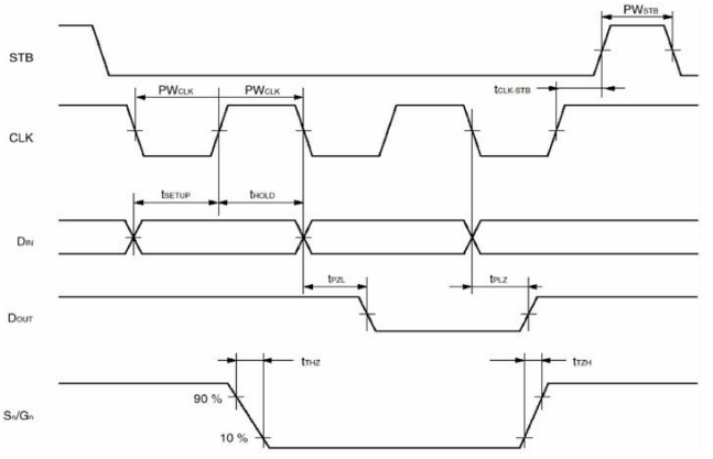
| Parametro |
min. |
max. |
Descrizione |
| TPLZ |
|
300ns |
transmit delay time |
| TPZL |
|
100ns |
|
| PWCLK |
400ns |
|
clock pulse width |
| PWSTB |
1us |
|
gate pulse width |
| Tsetup |
100ns |
|
data building time |
| Thold |
100ns |
|
data hold time |
| TIHZ |
|
120ns |
STB falling time |
| TTZH |
|
500ns |
STB rising time |
| Fmax |
|
1MHz |
clock frequency |
Display & LED.
You can control common cathode display:
Thus, to turn on the digit 0 it will be necessary to write 001111111111 (3Fh) in the desired register. The decimal point (dp) corresponds to bit7. Write 0 all segments will be turned off.
It is also possible to use a common anode display:
Typical hardware.
The TM1638 can control up to 80 LEDs or segments, which can be configured in a variety of ways.
There are a number of Chinese production modules available on the market with a number of LEDs, displays and keys, referring to the following three examples. As a common feature for this class of products, they are not accompanied by any documentation and it is necessary to do some research on the WEB to get more information.
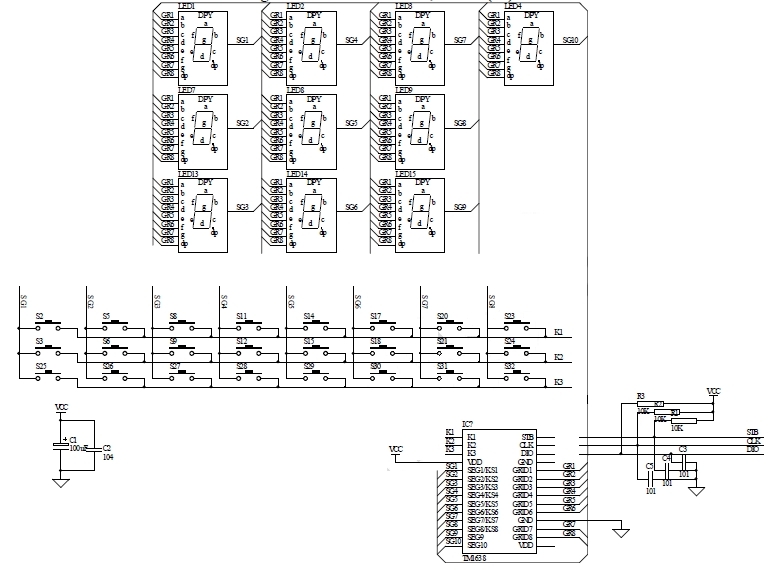
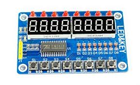
A typical TM1638 card, sold on many sites, has 8 digits of seven-segment, 8 two-tone LEDs and 8
buttons.
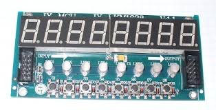 |
Note the 10-pin DIL connector that allows multiple modules to be cascaded: DIO and CLK are all connected, while each module depends on its own STB line.
The chain is made from flat ten-pole cables.
Here
is the wiring diagram.
|
| Funzione |
pin |
pin |
Funzione |
| Vcc |
1 |
2 |
GND |
| CLK |
3 |
4 |
DIO |
| STB0 |
5 |
6 |
STB1 |
| STB2 |
7 |
8 |
STB3 |
| STB4 |
9 |
10 |
n.c. |
|
The signals required for the local board are pin 1/2/3/3/4/5.
Pin 6/7/8/9 are the strobes for subsequent cards
|
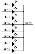
Each of the 7-segment displays can be accessed at an even address, where the 8 bits correspond to the segments + the dp.
Note that the TM1638 does not have a decoder and the value of each bit transmitted as given is returned to the corresponding segment.
|
b7 |
b6 |
b5 |
b4 |
b3 |
b2 |
b1 |
b0 |
 |
|
dp |
seg g |
seg f |
seg e |
seg d |
seg c |
seg b |
seg a |
Thus, for example, to obtain the digit 9 it will be necessary to switch on segments a, b, c, c, d, f, g, i. e. send the value 0001111111. By sending 1111111111, all segments (item 8) plus the decimal point will light up.
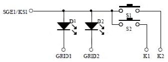
The two useful bits of the odd addresses are connected to the two-colour LEDs.
The following table shows the assignments for this type of card.
| Registro |
Comando
di
indirizzo |
Funzione |
LED |
| 00 |
0xC0 |
display 1 |
|
| 01 |
0xC1 |
LED 1 |
0x01 red
0x02 green |
| 02 |
0xC2 |
display 2 |
|
| 03 |
0xC3 |
LED 2 |
0x01 red
0x02 green |
| 04 |
0xC4 |
display 3 |
|
| 05 |
0xC5 |
LED 3 |
0x01 red
0x02 green |
| 06 |
0xC6 |
display 4 |
|
| 07 |
0xC7 |
LED 4 |
0x01 red
0x02 green |
| 08 |
0xC8 |
display 5 |
|
| 09 |
0xC9 |
LED 5 |
0x01 red
0x02 green |
| 0A |
0xCA |
display 6 |
|
| 0B |
0xCB |
LED 6 |
0x01 red
0x02 green |
| 0C |
0xCC |
display 7 |
|
| 0D |
0xCD |
LED 7 |
0x01 red
0x02 green |
| 0E |
0xCE |
display 8 |
|
| 0F |
0xCF |
LED 8 |
0x01 red
0x02 green |
The LEDs are connected to the SEG10:9 lines and therefore depend on odd registers, with bits b1:0.
In this case (bi-colour LED), bit b0 controls the red colour and b1 controls the green colour.
The bit set to 0 turns off the LED, while at 1 it turns on.
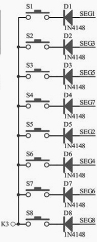 |
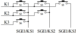
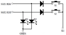
The buttons are connected between the common K3 and SEG8:1, as in the figure to the side.
Series diodes prevent the display from being disturbed if several keys are pressed
simultaneously.
From the connections it follows that the coding is the one visible in the following table:.
| b7 |
b6 |
b5 |
b4 |
b3 |
b2 |
b1 |
b0 |
|
| |
|
|
S5 |
|
|
|
S1 |
byte 1 |
| |
|
|
S6 |
|
|
|
S2 |
byte 2 |
| |
|
|
S7 |
|
|
|
S3 |
byte 3 |
| |
|
|
S8 |
|
|
|
S4 |
byte 4 |
|
So, if S1 is closed, the reading will make 0000000001 in the first byte and 0 in all the others.
If S8 is closed, the reading will make 0001000000 in the fourth byte and so on.
 |
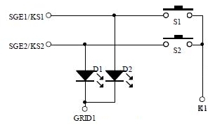
There are also cards with single-colour LEDs.
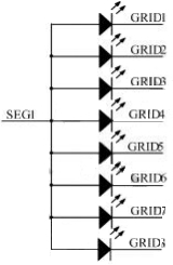
In this case, the LEDs are connected to GR8:1 and have SEG9 in common.
Then they are controlled by the b0 bit of the odd addresses (b0=1 LED on, b0=0 LED off).
Here too the buttons have in common K3 and the links seen above.
|
Here
is the wiring diagram..
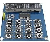 |
There are also modules with different display and button quantities, such as this one, with 8 digits and 16 buttons, but without additional
LEDs. |
These tabs allow you to add alerts and buttons to any project with negligible expense, since they have incredibly low costs, especially if sent directly from China.
Operating examples.
As an initial operation after applying voltage, it may be necessary to clear all memory locations of the TM1638, which may initially contain random values.
This is easily achieved by setting the automatic increment mode (0x40), selecting 0 as the starting address (0xC0) and sending the data 0 sixteen
times.
- STB low
- 0x40 ; Auto-address incremental writing command
- STB high
- STB low
- 0xC0 ; address of the first digit to the left
- 0x00 ; all segments and LEDs off
- repeat the data for another 15 times
- STB high
Note that STB opens and closes the communication, both for mode command output and
address/data sequence.
Now that the card is ready to work, you can send data for display.
For example, we write 8 in the last digit on the right and 1 in the first digit on the left.
Since these are two non-consecutive addresses, we use the single address mode.
The sequence to be sent will be as follows:
- STB low
- 0x44 ; single address mode
- STB high
- STB low
- 0xC0 ; address of the first digit
- 0x06 ; 00000110 segments b and c
on
- STB high
- STB low
- 0xCE ; address of the last digit
- 0x7F ; 01111111 all segments on
- STB high
Observe that STB opens and closes the communication, both for outputting the mode command and for the sequence of
address/data pairs.
Another example: we write the numbers from 1 to 4 in the first displays, turning on the decimal points and the LEDs alternately of different color:
- STB low
- 0x40 ; Auto-address incremental writing command
- STB high
- STB low
- 0xC0 ; address of the first digit
- 0x06 ; 00000110 segments b and c
on
- 0x01 ; LED red
- 0xDB ; 11011011
segments a,b,d,g,dp on
- 0x02 ; LED green
- 0xCF ; 01001111 segments
a,b,c,d,e,g on
- 0x01 ; LED red
- 0xB6 ; 10110110
segments b,c,e,f,dp on
- 0x02 ; LED green
- STB high
Note that, since the TM1638 does not have an encoder, it is not necessary to send the digits to be displayed, but the corresponding 7-segment mask, which can be obtained from a retlw
table.
If we want to turn on the third LED and fourth decimal point:
- STB low
- 0x40 ; Auto-address incremental writing command
- STB high
- STB low
- 0xC4 ; third LED address
- 0x02 ; LED green on
- 0x80 ; dp next display
on
- STB high
To read the status of the buttons, send the appropriate command (0x42) and then read 4
bytes.
The first byte contains the status of buttons S1 (bit 1) and S5 (bit 4), the second byte contains the status of buttons S2 (bit 2) and S6 (bit 5) and so on. If a bit is set to 1, it means that the corresponding button is pressed.
A delay of at least 1us must be entered between the reading of one byte and the next
- STB low
- 0x42 ; read key command
- Master DIO as input
- wait 1us
- read byte 1 and save
- read byte 2 and save
- read byte 3 and save
- read byte 4 and save
- STB high
- DIO Master side reconfigured as output
When reading the button status, the DIO line becomes an output driven by the TM1638 and the corresponding master pin must be an input. The clock is always supplied by the Master.
DRIVER.
Various examples of C libraries are available on the WEB.
An application example has been produced for the Assembly. Here you will find a version for Enhanced
Midrange.
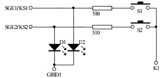
Some hardware notes. 1. - Input
RC On all Chinese 4-digit and TM1638 cards, 10k pull-up and 100pF capacitors are installed on the input lines.
It should be noted that DIO, in output, does not pilot the line at a high level, but is configured as an open drain and requires the pull-up.
The value of the capacitance is not negligible and influences the rise and fall times of the signals.
2. - Hardware of chinese modules
Modules with display, LEDs, buttons and TM1638 are available on the market at very low prices.
The costs are as low as ever, but, as for most Chinese products of this class, the technical documentation of these modules do not exist: there is not even a miserable leaflet to accompany the object, nor are there any information in this sense on most sites of the sellers, even if some, rare, have diagrams or even extensive documentation (but only in
Chinese...)
Even for the displays you may find it difficult to find a datasheet, even if only indicative. So, except for WEB searches, there is no information on how the components are connected and therefore the corresponding registers
In the case of common modules, such as those dashed before, connections can be traced back by analyzing the existing
drivers.
In the modules there may be no indication that LEDs are mono color; a generic differentiation can be made by observing the photos of the modules: red LEDs are only of this color, LEDs with white body are two-tone.
3. - Power supply One final note concerns the supply voltage: if TM1638 can be supplied from 3 to 5V, it is the minimum LED conduction voltage that determines the minimum supply value. Thus, blue LEDs will not be able to be powered at less than 5V.
Documentation.
|