Generate a sine with microcontroller.
A waveform can be generated by any microcontroller using a DA converter.
 |
Unfortunately, it is a device present only on some chips and, where there is not, the alternative is to use an external chip, which, in turn, requires a SPI or I2C communication, which has to be implemented.
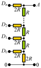
The most common solution becomes to use a R-2R network outside.
Here, however, we have the necessity of a number of digital I / O equal to the definition of the network: for 8-bit will have 8 pin
engaged.
When we are to have a smaller number of pins, as in the case of the chip in a container 8 pin, this is not possible and it is necessary to use a different
technique. |
We know that, in a PWM modulation where the frequency is kept fixed and varying the duty cycle, moves to 'output a variable percentage of energy.
We can use the PWM signal in different ways, of which the most common are:
- use the PWM directly for drive the load, also with a buffer, to vary, for example, brightness of the LED or speed
of motors
- or, by inserting a low pass filter which isolates only the DC component, obtaining a variable voltage. In this case, the low pass filter will eliminate any alternating component, including the fundamental
frequency.
But we can also apply a filter that eliminates the high harmonics of the fundamental, while maintaining this and pulling it out as alternating component with a constant frequency, the level of which will vary according to the variation of the duty
cycle.
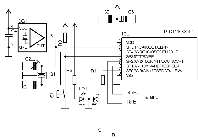
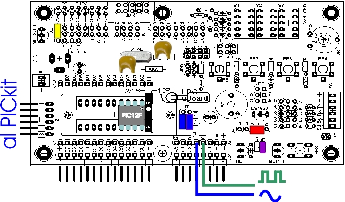
The CCP module / PWM is present on many PIC, also with the possibility of multiple channels; is also found in small 8-pin chip, like the 12F683, microcontroller Midrange fairly widespread and that we will use in this application. Obviously you can replicate it for any other PIC with CCP / PWM.
One may wonder what is the benefit of using the microcontroller to generate a waveform. This is essentially due to the high precision frequency that depends on the 'crystal oscillator clock. The sinusoid output will have the same precision clock oscillator, difficult to achieve with precision analog circuits, which require components of RC values are not always easily available.
Here, we want to get 1kHz, base frequency for a large number of measures.
The idea is taken from a work of Roman
Black.
The circuit
We can create a circuit based on these principles.
It uses a 20MHz crystal oscillator or, alternatively, an external oscillator. In the scheme are given both, but, of course, only one will be
wired.
The external oscillator, against a higher cost, provides greater accuracy and
stability.
A classic crystal + capacitors oscillator have a compensator to adjust the frequency. The values of the capacitors depends on the quartz used and are between 18 and 33pF; prototypes were used, with quartz from different manufacturers, the capacitors from NP0 22pF.
With the clock to 20 MHz, we have a cycle of education 200ns. This allows us to obtain a precise PWM from CCP module with a cadence of 20us.
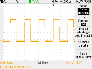
The program includes an auxiliary output to 50kHz that can be used, as we shall see, for the next filter. From the same output is also the possibility of obtaining an alternative 1MHz (duty cycle 40%),
both to facilitate the calibration that for general use. This function is achieved by closing the S1 button.
A two-color LED with two pins is used to report the mode of operation. When S1 is closed, the microcontroller port pin GP0 at high level, turning on the red LED (R) through
R1; the led light orange. When S1 is open, GP0 will be brought to 0, and only
the green LED (G) is on through R2.
The components are:
| R1 |
R2 |
R3 |
C1 |
C2 |
C3 |
C4 |
C5 |
Q1/QG1 |
S1 |
LED |
| 820 |
820 |
47k |
18-33p |
3-30p |
100n |
100n |
100u |
20MHz |
interr. |
bicol. |
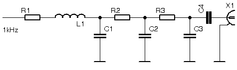
The signal at 1 kHz is sent to a low pass filter that suppresses the harmonics and the output of which will be found the sinusoid with minimal distortion.
A first solution is given by a series of RC filters:
This is three low pass the first of which also includes an inductance. The advantage is given by the zero consumption on 'power and by a relative low cost; despite a precise calculation requires values uncommon, you too can achieve positive results with easily obtainable components. By contrast, introduces a degree of attenuation. C4 is a non-polarized, which eliminates the continuous component.
The values are:
| R1 |
R2 |
R3 |
L1 |
C1 |
C2 |
C3 |
C4 |
| 330 |
330 |
820 |
2.2mH |
0.33uF |
68nF |
68nF |
10uF np |
The values are approximated to those of the most common commercial series.
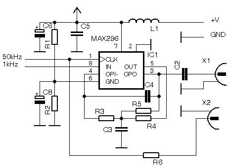
A second solution, a little more complex, is to use a digital filter. We can choose one of several integrated designed for this purpose, based on switched capacitor and produced by various manufacturers. Lend themselves well MAX295 / 296 Maxim, which have a ratio 50: 1 between clock frequency and frequency filtered.
Here we use a MAX296, Bessel's eighth order.
The power supply is filtered with a LG (L1 / C5 / C6) that separate very well the filter from digital noise induced on 'power.
PWM clock and are sent directly to the MAX; this is expected for a dual power supply, that, if desired implement, provides the best results. However, here the circuit is intended for a single power supply is necessary and a virtual ground formed by R1 / R2 / C8.
R6 is a protective resistor that separates the connector from the circuit X2.
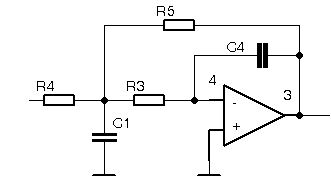
The MAX29x also incorporate an operational amplifier (pins 3-4) which is used as an additional low pass (Sallen-Key topology multiple feedback):
The components:
| R1 |
R2 |
R3 |
R4 |
R5 |
R6 |
C1 |
C2 |
C3 |
C4 |
C5 |
C6 |
C8 |
L1 |
| 10k |
10k |
16.5k |
14.7k |
14.7k |
50 |
22nF |
10uF
np |
100uF |
4nF7 |
10nF |
100uF |
4uF7
tant. |
1mH |
The resistor's values are approximated to those of the most common SND commercial
series
Development is possible with ease using the card LPCuB:
The filters are made externally on breadboard for a quickly modify of the components.
The final version may then be carried out on a specific printed circuit.
Software.
In the program, the PWM is supplied with the clock at 20MHz: for a loop, established from PR2, 100 clock pulses, we will obtain a frequency of 50kHz.
; initialize CCP module for PWM
; Microchip suggestion on data sheet
clrf
CCP1CON ; CCP Module is off
clrf
TMR2 ; clear Timer2
banksel PR2
movlw
(.100-1)
movwf
PR2
banksel GPIO
clrf
INTCON ; clear T0IF
banksel TRISIO
bcf
Sout ; make pin output
banksel GPIO
clrf
PIR1 ; clear peripheral interrupts Flags
; CCP1 ON, and set to PWM mode
movlw
b'00001101'
movwf
CCP1CON
movlw
.52 ; first value from the table
movwf
CCPR1L
; and start TRM2
movlw
b'00000100'
movwf
T2CON |
For each output pulse of the PWM signal is associated with a different duty cycle value, taken from a table of 50 steps, thereby obtaining a sinusoidal variation of the same duty cycle between about 15 and 85% each kilohertz.
The Directive dt
compiles quickly retlw
table.
; "harmonic compensated" sine table
sinetable addwf PCL,f
dt 52,57,62,66,70,74,77,80,82,84,85,86,86
dt 86,85,83,81,78,75,72,69,65,61,56,52
dt 48,44,39,35,31,28,25,22,19,17,15,14,14
dt 14,15,16,18,20,23,26,30,34,38,43,48 |
At the same time it generates a square wave signal of 50 kHz which will be used for the digital filter. This signal has a duty cycle of 50% as active filters require this to work best; it is simply obtained within the loop update of the PWM, with a pulse at high level of 50 instruction cycles.
; 50kHz pulse
bsf
Faux ; pulse start
movlw 0x10
; 49 cycles
movwf d1
dcyc decfsz d1, f
goto
dcyc
bcf
Faux ; pulse end
|
Given that the next pulse will be triggered at the end of a PWM cycle that lasts 100 instruction cycles, here we have the correct duty
cycle.
An added bonus is supplied from the switch S1, the closing of which deflects the 'running on a stretch of program that generally a square wave with duty cycle of 40% and a frequency of 1MHz, which can be used for the calibration of' oscillator. L 'asymmetry is due to the necessity of the test on the state of the switch that switches the manner and to the loop, since the instruction cycle is 200ns.
; Calibrate mode: make a 1MHz fixed freq
on pin Faux
; 5 instructions per cycle,
; output squarewave 1MHz with 40% on duty.
cal_mode:
clrf
CCP1CON ; CCP1 module is turned OFF
; MHz mode - LED red on
LEDRED
loop_1MHz:
bsf
Faux ; output high
nop
bcf
Faux ; output low
btfsc btn
; test switch for SINE mode
goto done_1MHz
; switch hi - exit go to SINE mode
bsf
Faux ; no - output high
nop
bcf
Faux ; output low
goto
loop_1MHz ; loop
done_1MHz:
; out from MHz mode
goto
sine_mode ; back to sine mode |
The switch is also equipped with a debounce time, to avoid the bounces generate random states of outputs.
The two-color LED is controlled depending on the position of S1.
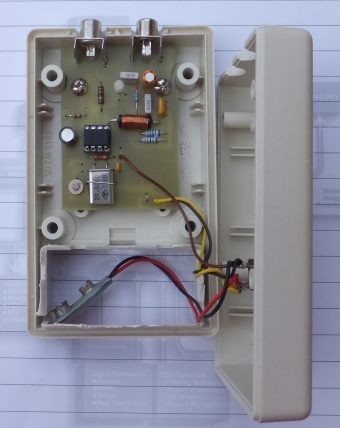
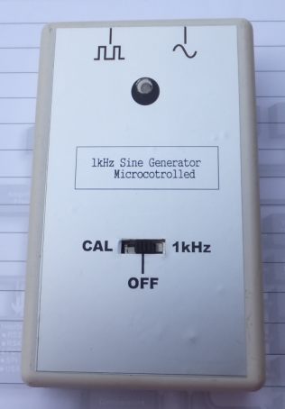
The box.
Was made a version portable, battery.
Here, 4 NiMH batteries are used I provide a variable voltage between 4.8V (loads) and 4.4V (discharges), which within the capabilities of the microcontroller, although it is likely that the variation of the supply voltage reflects poorly on the
stability. It was used the passive filter, which does not consume power, extending battery life
(the entire circuit draws approximately 7.5 mA).
The oscillator is a crystal and the capacitive trimmer allows an adjustment of the
frequency.
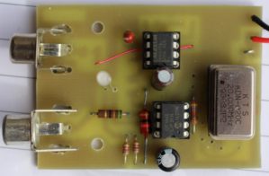
A version of "counter" is easily accomplished with the usual 78L05 regulator and an external wall plug. Here you have implemented the digital filter and the oscillator clock is an
external 14-pin module.
The firmware is identical for both versions; goes only modified the initial config where you want to use the external oscillator:
; config per oscillatore a
quarzo
__config _HS_OSC & _WDTE_OFF & _PWRTE_ON & _BOREN_OFF & _IESO_OFF & _FCMEN_OFF & _MCLRE_OFF
; config per oscillatore esterno
__config _EC_OSC & _WDTE_OFF &
_PWRTE_OFF & _BOREN_OFF & _IESO_OFF & _FCMEN_OFF & _MCLRE_OFF |
The output signal from the PWM should be considered in its alternating component at the fundamental frequency. However, since the variation of the duty cycle is not continuous, but in steps, sensitive components are introduced at multiple frequencies, which are to be torn down by the low pass filter. In particular, the second harmonic is the most obvious, while the sampling errors of the above values are
secondary.
Both the passive filter that makes the active satisfactory results.
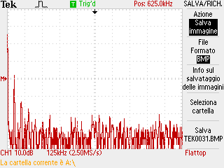
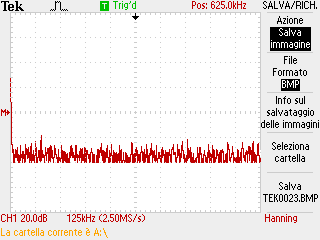
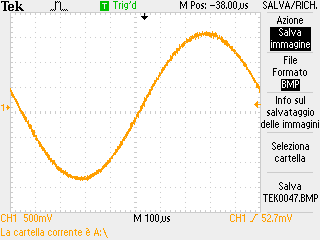
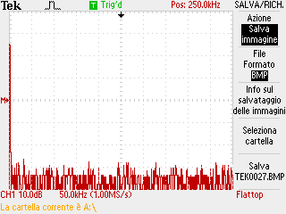
Passive filter, first cell RLC and output. Next, the FFT data from 'oscilloscope.
All 'beginning of the filter you notice the strong presence of harmonics, which are then reduced to' output.
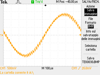
The sine wave output amplitude to a vacuum of about 1.4V.
Tweaking the equalizer you can adjust the frequency of 'oscillator. With the tools available has been recognized as the best value of the frequency of
1.000.070 MHz.
Here we see the 'output and the 50kHz to 1MHz:
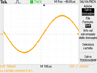
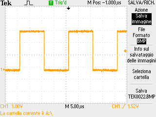
This is the output waveform of the digital filter:.
C vs. Asm
The
original idea has a C source in which there is a significant intrusion of Assembly.
This is because it is not possible to use the C in order to ensure a total control at the level of individual instructions as in this case, where the timings, for example, that to generate the MHz, are
stringent.
Assembly offers a full control of the times, so that, for example, the' insertion of the clock at 50kHz is extremely simple, while the C would have required more sections asm.
Here we preferred an approach entirely Assembly, which is much better calibrated on the application, which does not require complex calculations or logical structures, but only an optimal management of the bits of I / O. And, for what concerns the audit logs of the CCP module / PWM, there is no real difference between C and Assembly in the form and in the understanding of the
source.
As a bonus, the 'executable produced by the Assembly source size is significantly smaller and requires less RAM.
Finally, one can notice that, for programs where you have to do primarily with I / O and SFR and must comply timing critical, l 'approach in C is not always the best one, and should be reserved to other areas, especially in small PIC with limited resources and little optimized for this
language.
The source was compiled for the 12F683, but is adaptable with great ease to any other PIC module equipped CCP / PWM, simply by adjusting the schedule to access the digital I / O (excluding the alternate functions), while the management of the PWM remains essentially unchanged through other Midrange, Enhanced Midrange and even PIC18F. It 'also easily adaptable to 10F32x, who MSSP and external clock input, or to give up the auxiliary clock indication LEDs (due to the low number of
pins).
And, given the simplicity of the source, it will not be difficult to overtake even Microcontrollers other manufacturers.
The principle may be applied to obtain different values the of the output frequency, by modifying the clock and / or the PWM.
The Assembly Source.
;******************************************************************************
; Sine1kHz.asm Precision 1kHz sinewave generator
; from an idea of www.RomanBlack.com/
;
; PIC 12F683 - 20MHz xtal
;-----------------------------------------------------------------------------
; I/O pins;
;
#define LED GPIO,GP0 ; Out LED Red
#define Faux GPIO,GP1 ; Out Faux
#define Sout GPIO,GP2 ; Out CCP1
#define btn GPIO,GP3 ; In button
; GP4 oscout
; GP5 oscin
;--------------------------------------------------------------------
;
LIST p=12F683 r=DEC
#include <p12F683.inc>
; for chrystal oscillator
__config _HS_OSC & _WDTE_OFF & _PWRTE_ON & _BOREN_OFF & _IESO_OFF & _FCMEN_OFF & _MCLRE_OFF
; for external oscillator module
; __config _EC_OSC & _WDTE_OFF & _PWRTE_OFF & _BOREN_OFF & _IESO_OFF & _FCMEN_OFF & _MCLRE_OFF
;*********************************************************************
; Data RAM area
CBLOCK 0x20
pwmstep ; PWM step 0-49
debounce ; debouncing switch input
d1 ; temporary for delay
ENDC
;********************************************************************
; LOCAL MACROS
; CFLSB Compare File to Literal and Skip if Below
; Compare register with literal and jump next line if
; file < literal
CFLSB MACRO file,lit
movlw (255-lit+1) ; W = -lit
addwf file,W
; W = file + W = file + (-lit)
skpnc
; C=0 for file<lit, than skip next line
ENDM
; C=1 for file>=lit, than execute next line
LEDGREEN MACRO
bcf LED
ENDM
LEDRED MACRO
bsf LED
ENDM
;=====================================================================
; MAIN
RESVEC ORG 0x00
Main goto init
; "harmonic compensated" sine table
sinetable addwf PCL,f
dt 52,57,62,66,70,74,77,80,82,84,85,86,86
dt 86,85,83,81,78,75,72,69,65,61,56,52
dt 48,44,39,35,31,28,25,22,19,17,15,14,14
dt 14,15,16,18,20,23,26,30,34,38,43,48
;--------------------------------------------------------------------
init:
; preload GPIO output latch
movlw 0
movwf GPIO
;comparators OFF, all pins digital
movlw b'00000111'
movwf CMCON0
; analog off and all possible as out
banksel ANSEL
clrf TRISIO
clrf ANSEL
; TMR0 not used, but clear T0CKI
movlw b'10001000'
movwf OPTION_REG
banksel GPIO
; setup any variables before main loop
clrf pwmstep
clrf debounce
;--------------------------------------------------------------------
; Sine mode: use PWM to make the sine out pin
sine_mode:
; LED green is on, red is off
LEDGREEN
; initialize CCP module for PWM
; Microchip suggestion on data sheet
clrf CCP1CON ; CCP Module is off
clrf TMR2
; clear Timer2
banksel PR2
movlw (.100-1)
movwf PR2
banksel GPIO
clrf INTCON ; clear T0IF
banksel TRISIO
bcf Sout
; make pin output
banksel GPIO
clrf PIR1
; clear peripheral interrupts Flags
; CCP1 ON, and set to PWM mode
movlw b'00001101'
movwf CCP1CON
movlw .52
; first value from the table
movwf CCPR1L
; and start TRM2
movlw b'00000100'
movwf T2CON
; loop: load new PWM value every TMR2 cycle
slp0 incf pwmstep,f ; inc to next step in sinewave
CFLSB pwmstep, .50 ; sine has 50 steps
clrf pwmstep
movf pwmstep,w ; read new PWM value
call sinetable ; from sinetable
slp1 btfss PIR1,TMR2IF ; wait for TMR2 cycle to restart
goto slp1
movwf CCPR1L
; load new value
bcf PIR1,TMR2IF ; clear TMR2 int flag
; 50kHz pulse
bsf Faux
movlw 0x10
;49 cycles
movwf d1
dcyc decfsz d1, f
goto dcyc
bcf Faux
; pulse end
; also check for switch being low, if so go to calibrate mode
btfsc btn
goto slp2
incf debounce,f
; if debounce > 250 goto cal_mode.
CFLSB debounce, .250
goto cal_mode
goto slp0
;else debounce = 0;
slp2 clrf debounce
goto slp0
; back to loop
;--------------------------------------------------------------------
; Calibrate mode: make a 1MHz fixed freq out pin Faux
; 5 instructions per output cycle,
; output squarewave 1MHz with 40% on duty.
cal_mode:
; CCP1 module is turned OFF
clrf CCP1CON
; CAL mode LED red is on
LEDRED
loop_1MHz:
bsf Faux
; output high
nop
bcf Faux
; output low
btfsc btn
; test switch for SINE mode
goto done_1MHz ; switch HI, so exit this mode and go back to SINE
bsf Faux
; output high
nop
bcf Faux
; output low
goto loop_1MHz ; loop
done_1MHz:
; out from cal_mode
goto sine_mode ; cal mode is done, back to sine mode
;-----------------------------------------------------------------------------
END |
|